|
#2
February 1st, 2016, 09:02 AM
| |||
| |||
| Re: IIT Delhi SEM Schedule
Scanning Electron Microscope Central Facility (SEMCF) is One Such Facility. All Students, Researchers and Faculty Members From Various Science and Engineering Departments of the Institute are free to Avail the Services of SEMCF as per the Guidelines laid by the SEM user Committee of the institute. These Guidelines are Regularly Reviewed from Time To time. Zeiss EVO 50 & EVO 18 Special The SEM Central Facility at IIT Delhi has recently acquired a new ZEISS EVO Series Scanning Electron Microscope EVO 50 and EVO 18. The ZEISS EVO 50 is a versatile analytical microscope with a large specimen chamber. Essential Specification: EVO 50: Resolution 2.0nm@ 30kV (SE with LaB6 option ) Acceleration Voltage 0.2 to 30 kV Magnification 5x to 1,000,000x Field of View 6 mm at the Analytical Working Distance (AWD) X-ray Analysis 8.5 mm AWD and 35° take-off angle Available Detectors SE in HV - Everhart-Thornley SE in VPSE BSD in all modes - quadrant semiconductor diode Some Features of EDX Analysis of known or Unknown Materials : Qualitative and quantitative analysis for all elements from carbon upwards in the periodic table Quantitative analysis of homogenous bulk materials having features = 2 µm Qualitative analysis of features = 0.2 µm Detection limits typically 0.1 – 100 Wt% for most elements Multi-element X-ray mapping and line scans Particle analysis – Detection, analysis, morphology and size. For SEM Schedule Calander Here I am Sharing Image of this page 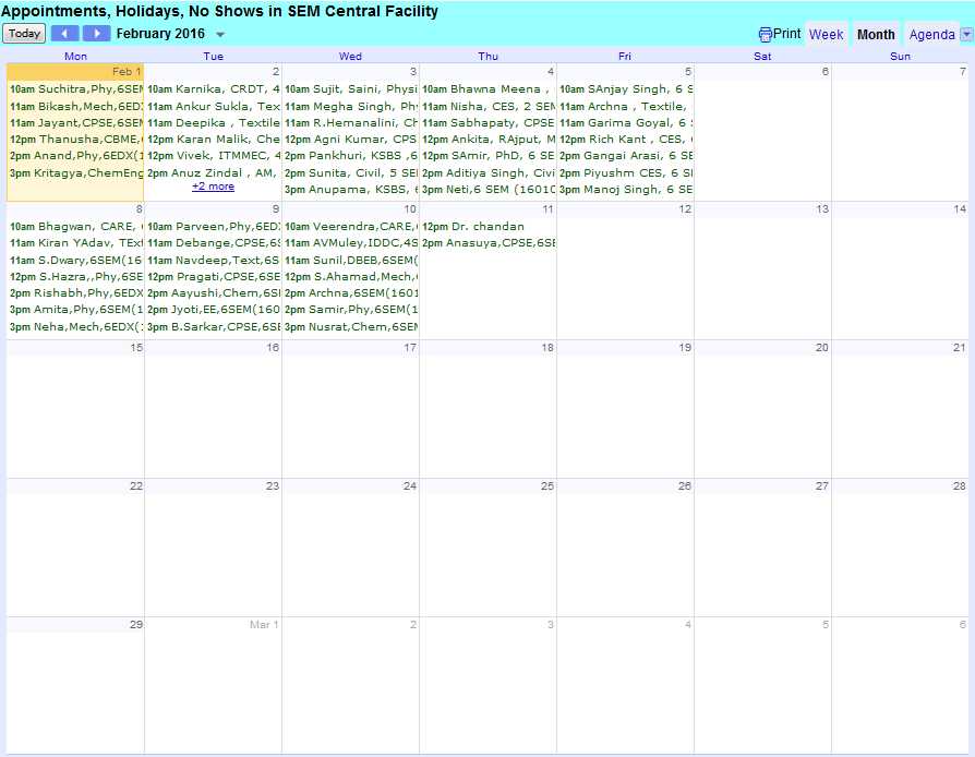 Contact No : 011 2659 7135 Address : Indian Institute of Technology Delhi Hauz Khas New Delhi, Delhi 110016 |