|
#3
February 14th, 2017, 11:24 AM
| |||
| |||
| Re: NITP Training
The National Institute of Technology Patna is offers training seminars on Federal Benefits, Financial Planning, and Thrift Savings Plan Options/Investments for employees at all stages of their Federal careers: New Employees, Mid-Career Employees, and Pre-Retirement Employees. The seminars address the Federal Employees Retirement System (FERS), the Civil Service Retirement System (CSRS) as well as the special retirement provision for law enforcement officers, firefighters, and air traffic controllers, when applicable. Training from of National Institute of Technology Patna 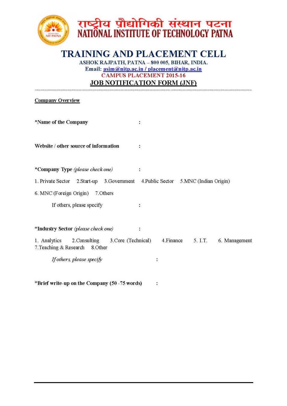 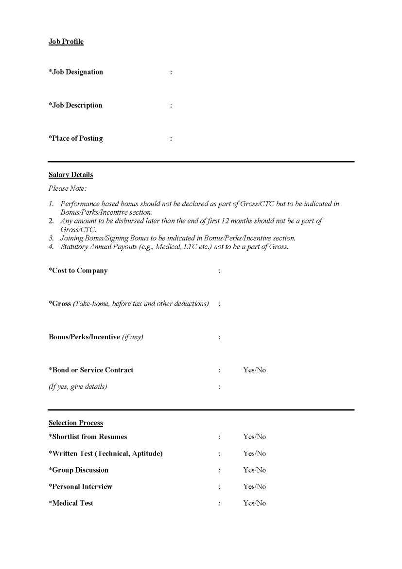 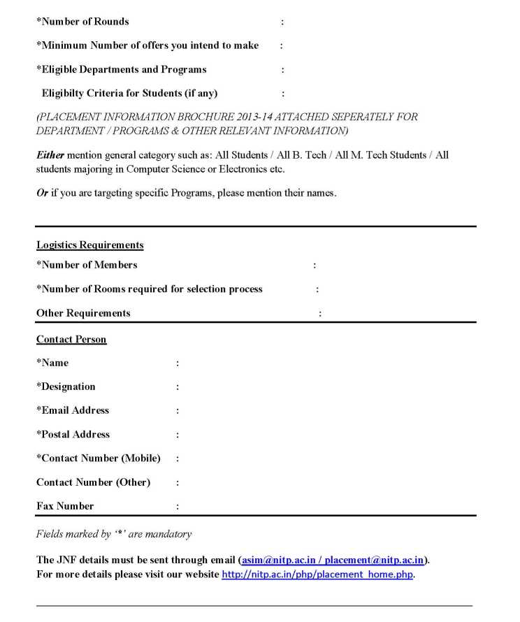 VLSI Design training program: ( L - 25 hrs., P - 15 hrs.) Course Outcome: Upon successful completion of this course, students should be able to understand the following: Microcontroller Organization and Architecture (ARM.8051) Understand the design rules and layout diagram. Understand the design of CMOS Memories. Understand design issues at the layout, transistor, logic, and register transfer levels. Analyse the physical design process of VLSI design flow. Theory (L - 25 hrs.) S.no Topic Lecture(hrs) 1 Introduction to VLSI design 1 2 Introduction to CMOS Technology, device characteristics 2 3 Analysis of CMOS logic Circuits(inverter, NAND gate, NOR gate) 3 4 Layout design rules 1 5 Advanced Techniques in CMOS logic circuit 3 6 Memories: Static RAM; SRAM arrays; Dynamic RAMs; 4 7 ROM arrays; Logic arrays, 1 8 Timing issues in VLSI system design CMOS Testing 3 9 Verilog Hardware Description language: Overview of digital design with Verilog HDL 1 10 Hierarchical modelling concepts; Modules and port definitions; 1 11 Gate level modelling; Data flow modelling; Behaviouralmodelling; 3 12 Task & functions; Test bench Laboratory 2 Total lecture (hrs.) 25 Address: National Institute of Technology Patna Patna, Bihar (800005), India Phone: +91-0612-237 1715 / 237 2715 FAX : +91-0612-2670631 , 0612-2660480 |