|
#2
February 8th, 2016, 08:09 AM
| |||
| |||
| Re: Syllabus M.Tech. VLSI Nagpur University
I have knowledge about the M.Tech. Syllabus at VLSI Nagpur University. So here I am providing you information about syllabus, as you want. Here I am providing you a file, which is containing; Nagpur University M. Tech. (VLSI) syllabus First Semester Syllabus 1FUV01 VLSI SUBSYSTEM DESIGN Section A Material Model Electrical Properties, Junction Diode. MOS transistor Operation Modes Threshold Voltage: Metal and Polysilicon Trapped Charge Implants Strong Inversion: Charge Modeling Constant Vt model: NMOS/PMOS transistors. I/V characteristics, Sign Conventions parasitic Bipolar Transistors CMOS Latch-up Analysis (D.C. and transient), Device capacitance and Charge Storage in MOS NMOS/CMOS circuit analysis, Small signal amplifier model Miller Effect. Layout / Fabrication, Diffusion / Implants / Wires, NMOS / CMOS Processes SCMOS Design Rules – special derivation self-aligned processes Resistor / Capacitor Layout, Logic Level Design, Cube Decomposition, Realization of Duals for CMOS Euler path layout, Topological Considerations. Don‟t Cares and Redundancy, layout Parasitic Reduction. Section B MOS Logic Families: Propagation Delay for CMOS/NMOS/PNMOS, Layout Capacitance / Resistance. Estimation; Gain effects; MOS Performance Estimation, Buffers/Capacitive Loading, Power Dissipation : Transient Optimization, Sidewall/2-d and 3-d effects: Cross-talk Fringing, Ball-park numbers for process Estimation Scaling CMOS Design Optimization: High-Speed Logic Strategies. Interconnection. Distributed R/C cross/talk, Noise, Clocking Strategies, Sub-System Design and Partitioning Dynamic Logic, Dynamic Circuits, Stored Charge and timing. Domino Logic, Switched Capacitor and Charge Flow circuits, pass-Transistor logic (CPL). Data-Path and Memory Circuits : Static/Dynamic memories, Ancillary memory Analog Circuits. MODELLING OF DIGITAL SYSTEM – 1 Section A Programming Technologies – ROMs & EPROMs PLA . PAL gate Arrays Programmable gate arrays and applications, Antifuse FPGA, Synthesis methods for FPGA. Hardware Description Language. Design entities, architecture Bodies, Block Statements, processes data types. Operators . Classes of Objects, Attributes, Functions and Procedures, Packages Control Statements. Behaviour modeling.- Process Statement, Assertion Statement, Sequential wait Statement, Formatted ASCII I/O Operations Structural Modeling ; parts Library wiring of Primitives. Wiring of Iterative networks. Modeling a test bench. Section B Chip Level Modeling : Chip level modeling structures modeling delay, process model graphs, Functionally partitioned models, Timing Assertion, Setup & Hold time for clocked devices, Design rule checks System Modeling : Modeling system interconnection, general model for signal interconnection, Multiplexing of signals. Multiple valued logic. Processor model. RAM model. UART model, Parallel I/O Ports, Interrupt controller Simulation with the physical model, simulation, writing test bench, converting real and interconnection, Multiplexing of signals. Multiple valued logic. Processor model. RAM model. UART model, Parallel I/O Ports, Interrupt controller. Simulation with the physical model, simulation, writing test bench, converting real and integer to time. Dumping results into text file, reading vectors from text file, test bench example. Address Nagpur University Chhatrapati Shivaji Maharaj Administrative Premises, Ravindranath Tagore Marg Nagpur, Maharashtra 440001 Syllabus m.tech. VLSI Nagpur University 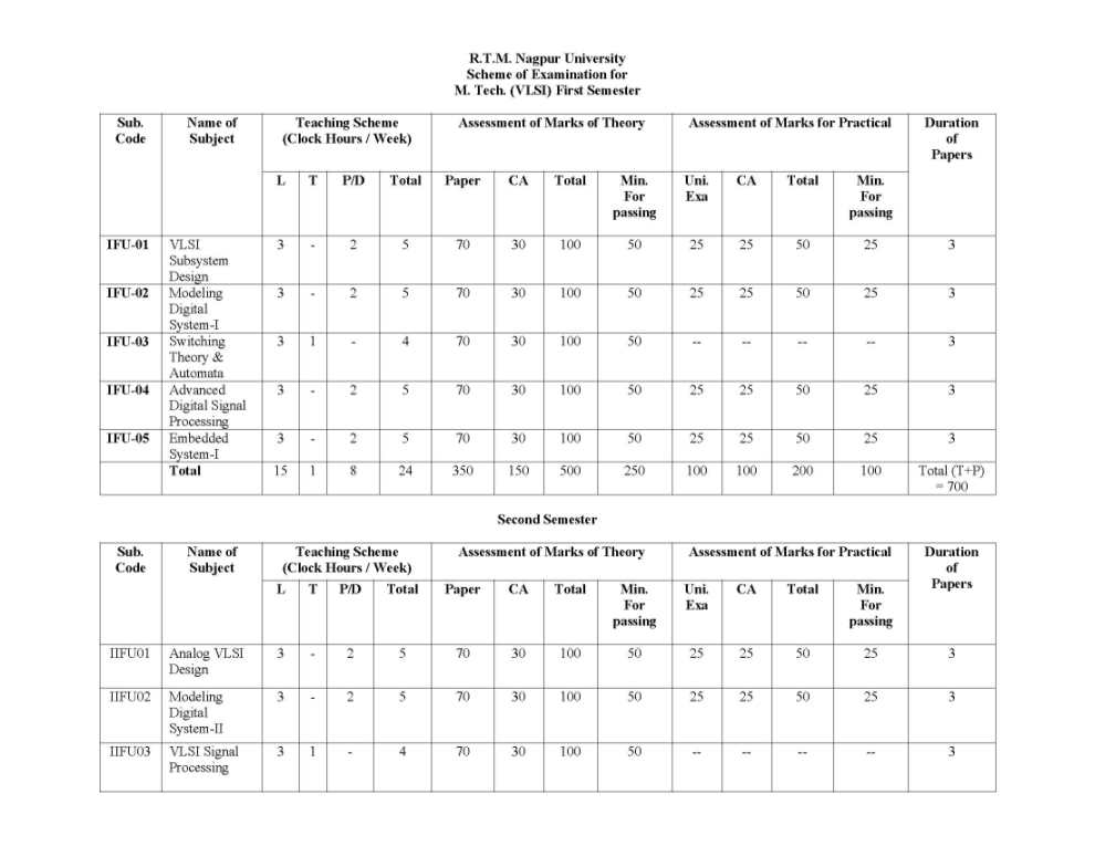   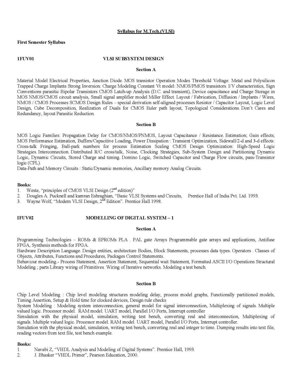  |